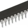

CD4724BE, Защелка, CD4724, Адресуемая, Стандартный, 50 нс, 6.8 мА, DIP
140,00 ₽
Адресуемый 8-битный latch с сериальным входом и параллельным выходом, удерживающий данные в регистре. Вход данных происходит в бит, адресованный A0, A1, A2, … Купить от FedExpert
The CD4724BE is a 8-bit Addressable Latch with serial-input parallel-output storage register that can perform a variety of functions. Data are inputted to a particular bit in the latch when that bit is addressed (by means of input A0, A1, A2) and when WD is at a low level. When WD is high, data entry is inhibited, however, all 8 outputs can be continuously read independent of WD and address inputs. A master RESET input is available, which RESETs all bits to a logic 0 level when RESET and WD are at a high level. When RESET is at a high level and WRITE RESET is at a low level, the latch acts as a 1-of-8 demultiplexer, the bit that is addressed has an active output which follows the data input, while all unaddressed bits are held to a logic 0 level.
• Serial data input
• Active parallel output
• Storage register capability
• Master clear
• Can function as demultiplexer
• Standardized, symmetrical output characteristics
• 100% Tested for quiescent current at 20V
Полупроводники — МикросхемыЛогикаТриггеры-защелки
Технические параметры
| Выходной Ток | 6.8мА |
| Минимальная Рабочая Температура | -55 C |
| Максимальная Рабочая Температура | 125 C |
| Максимальное Напряжение Питания | 18В |
| Минимальное Напряжение Питания | 3В |
| Количество Выводов | 16вывод(-ов) |
| Тип Выхода Микросхемы | стандартный |
| Количество Бит | 8бит |
| Задержка Распространения | 50нс |
| Стиль Корпуса Микросхемы Логики | dip |
| Тип Защелки | Адресуемая |
| Базовый Номер / Семейство Логики | CD4724 |
| Базовый Номер Микросхемы Логики | 4724 |
| Семейство Логической Микросхемы | CD4000 |
| Вес, г | 3.969 |
Похожие товары

Texas Instruments
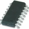
SN74AS373N, Защелка, 74AS373, Прозрачная D Типа, С Тремя Состояниями, 6 нс, 24 мА, DIP
Texas Instruments
Texas Instruments
SN74ABT16373ADL, Защелка, 74ABT16373, Прозрачная, С Тремя Состояниями, 3.7 нс, 64 мА, SSOP
Texas Instruments
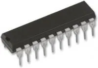
CD74HCT533E, Защелка, семейство HCT, 74HCT533, Прозрачная, С Тремя Состояниями, 14 нс, 6 мА, DIP

Texas Instruments
CD74ACT573M, Защелка, 74ACT573, Прозрачная, С Тремя Состояниями, 9.4 нс, 24 мА, SOIC
Texas Instruments
SN74ABT573ADW, Защелка, 74ABT573, Прозрачная, С Тремя Состояниями, 3.2 нс, 64 мА, SOIC
Texas Instruments