
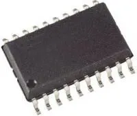
SN74HC259D, Защелка, семейство HC, 74HC259, Адресуемая, Стандартный, 28 нс, 5.2 мА, SOIC
42,00 ₽
High-speed, 8-bit addressable latch for versatile digital storage. Купить от FedExpert
The SN74HC259D is a 8-bit Addressable Latch designed for general-purpose storage applications in digital systems. Specific uses include working registers, serial-holding registers and active-high decoders or demultiplexers. They are multifunctional devices capable of storing single-line data in eight addressable latches and being a 1-of-8 decoder or demultiplexer with active-high outputs. Four distinct modes of operation are selectable by controlling the clear (CLR) and enable (G) inputs. In the addressable-latch mode, data at the data-in terminal is written into the addressed latch. The addressed latch follows the data input, with all unaddressed latches remaining in their previous states. In the memory mode, all latches remain in their previous states and are unaffected by the data or address inputs.
• Wide operating voltage range
• Outputs can drive up to 10 LSTTL loads
• Low power consumption
• 14ns Typical TPD
• ±4mA Output drive at 5V
• 1µA Maximum low input current
• Asynchronous parallel clear
• Active-high decoder
• Enable input simplifies expansion
• Green product and no Sb/Br
Полупроводники — МикросхемыЛогикаТриггеры-защелки
Технические параметры
| Выходной Ток | 5.2мА |
| Минимальная Рабочая Температура | -40 C |
| Максимальная Рабочая Температура | 85 C |
| Максимальное Напряжение Питания | 6В |
| Минимальное Напряжение Питания | 2В |
| Количество Выводов | 16вывод(-ов) |
| Тип Выхода Микросхемы | стандартный |
| Количество Бит | 8бит |
| Задержка Распространения | 28нс |
| Стиль Корпуса Микросхемы Логики | SOIC |
| Тип Защелки | Адресуемая |
| Базовый Номер / Семейство Логики | 74HC259 |
| Базовый Номер Микросхемы Логики | 74259 |
| Семейство Логической Микросхемы | 74HC |
| Вес, г | 0.335 |
Похожие товары

Texas Instruments
CD4724BE, Защелка, CD4724, Адресуемая, Стандартный, 50 нс, 6.8 мА, DIP
Texas Instruments
SN74ACT573PW, Защелка, 74ACT573, Прозрачная, С Тремя Состояниями, 12 нс, 24 мА, TSSOP

Texas Instruments
SN74AC573PWR, Защелка, 74AC573, Прозрачная D Типа, С Тремя Состояниями, 11.5 нс, TSSOP
Texas Instruments
Texas Instruments
Texas Instruments
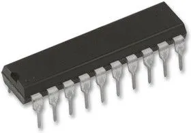
CD74HC259E, Защелка, семейство HC, 74HC259, Адресуемая, Стандартный, 15 нс, 5.2 мА, DIP