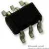

SN74LVC1G374DCKR, Триггер, неинвертированный на 3 состояния, положительный фронт, 74LVC1G374, D, 3 нс, 175 МГц, SC-70
26,00 ₽
High-speed, 3-state D flip-flop for low-voltage, high-capacity loads. Ideal for buffers, I/O ports, and bus drivers. Купить от FedExpert
The SN74LVC1G374DCKR is a single D-type Flip-flop designed for 1.65 to 5.5V VCC operation. It features a 3-state output designed specifically for driving highly capacitive or relatively low-impedance loads. This device is particularly suitable for implementing buffer registers, input/output (I/O) ports, bidirectional bus drivers and working registers. On the positive transition of the clock input, the Q output is set to the logic level set up at the data (D) input. A buffered OE input can be used to place the output in either a normal logic state or the high-impedance state. In the high-impedance state, the output neither loads nor drives the bus lines significantly. The high-impedance state and increased drive provide the capability to drive bus lines without interface or pull-up components. OE does not affect the internal operations of the flip-flop. Old data can be retained or new data can be entered while the outputs are in the high-impedance state.
• Supports down translation to VCC
• Ioff Supports live insertion, partial-power-down mode and back-drive protection
• Latch-up performance exceeds 100mA per JESD 78, class II
• 10µA Maximum low power consumption
• ±24mA Output drive at 3.3V
• Green product and no Sb/Br
Полупроводники — МикросхемыЛогикаТриггеры
Технические параметры
| Минимальная Рабочая Температура | -40 C |
| Максимальная Рабочая Температура | 125 C |
| Частота | 175МГц |
| Максимальное Напряжение Питания | 5.5В |
| Минимальное Напряжение Питания | 1.65В |
| Количество Выводов | 6вывод(-ов) |
| Тип Выхода Микросхемы | С Тремя Состояниями Неинвертирующий |
| Задержка Распространения | 3нс |
| Стиль Корпуса Микросхемы Логики | sc-70 |
| Тип Триггера | D, Положительный Фронт |
| Базовый Номер / Семейство Логики | 74LVC1G374 |
| Базовый Номер Микросхемы Логики | 741G374 |
| Семейство Логической Микросхемы | 74LVC |
| Вес, г | 0.045 |
Похожие товары

Texas Instruments
Texas Instruments
CD74HC107E, Триггер, 74HC107, JK, 14 нс, 60 МГц, 5.2 мА, DIP
Texas Instruments
Texas Instruments
Texas Instruments
SN74ABT377AN, Триггер, 74ABT377, D, 4.5 нс, 150 МГц, 64 мА, DIP