


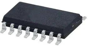
CD4094BNSR, Регистр сдвига, регистр сдвига и хранения, CD4094, Последовательный в Параллельный, 1 Элемент
36,00 ₽
8-bit Shift & Store Bus Register: Parallel outputs, serial inputs, ideal for cascading. Купить от FedExpert
The CD4094BNSR is a 8-stage CMOS shift-and-store Bus Register having a storage latch associated with each stage for strobing data from the serial input to parallel buffered 3-state outputs. The parallel outputs may be connected directly to common bus lines. Data is shifted on positive clock transitions. The data in each shift register stage is transferred to the storage register when the STROBE input is high. Data in the storage register appears at the outputs whenever the OE signal is high. Two serial outputs are available for cascading a number of CD4094B devices. Data is available at the QS serial output terminal on positive clock edges to allow for high-speed operation in cascaded systems in which the clock rise time is fast. The same serial information, available at the QS terminal on the next negative clock edge, provides a means for cascading CD4094B devices when the clock rise time is slow.
• Separate serial outputs synchronous to both positive and negative clock edges for cascading
• 5MHz at 10V Typical medium speed operation
• Standardized, symmetrical output characteristics
• 100% Tested for quiescent current at 20V
• Meets all requirements of JEDEC tentative standard no. 13B
• 3-state Parallel outputs for connection to common bus
• Green product and no Sb/Br
Полупроводники — МикросхемыЛогикаСдвигающие Регистры
Технические параметры
| Количество элементов | 1 Элемент |
| Минимальная Рабочая Температура | -55 C |
| Максимальная Рабочая Температура | 125 C |
| Максимальное Напряжение Питания | 18В |
| Минимальное Напряжение Питания | 3В |
| Количество Выводов | 16вывод(-ов) |
| Тип Выхода Микросхемы | С Тремя Состояниями |
| Стиль Корпуса Микросхемы Логики | sop |
| Функция Сдвига Регистра | Последовательный в Параллельный |
| Базовый Номер / Семейство Логики | CD4094 |
| Базовый Номер Микросхемы Логики | 4094 |
| Семейство Логической Микросхемы | CD4000 |
| Количество Бит на Элемент | 8бит |
| Вес, г | 0.253 |
Похожие товары

Texas Instruments
CD74HC299E, Регистр сдвига, 74HC299, Универсальный, 1 Элемент, 8 бит, DIP, 20 вывод(-ов)
Texas Instruments
Texas Instruments