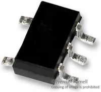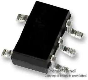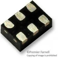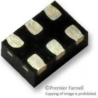

74LVC2G17GW,125, Буфер, триггер Шмитта, 1.65В до 5.5В, SC-88-6
26,00 ₽
Schmitt Trigger Buffer: Converts slow signals to crisp outputs, compatible with 3.3/5V devices, power-down protected. Купить от FedExpert
The 74LVC2G17GW, 125 is a dual non-inverting Buffer with Schmitt trigger input. It is capable of transforming slowly changing input signals into sharply defined, jitter-free output signals. Inputs can be driven from either 3.3/5V devices. This feature allows the use of these devices as translators in a mixed 3.3 and 5V environment. This device is fully specified for partial power-down applications using IOFF. The IOFF circuitry disables the output, preventing the damaging backflow current through the device when it is powered down.
• High noise immunity
• CMOS low-power consumption
• Direct interface with TTL levels
• Complies with JEDEC standard
• 5V Tolerant input/output for interfacing with 5V logic
• Latch-up performance exceeds 250mA
• ±24mA Output drive
Полупроводники — МикросхемыЛогикаБуферы, Приемопередатчики и Линейные Драйверы
Технические параметры
| Минимальная Рабочая Температура | -40 C |
| Максимальная Рабочая Температура | 125 C |
| Максимальное Напряжение Питания | 5.5В |
| Минимальное Напряжение Питания | 1.65В |
| Количество Выводов | 6вывод(-ов) |
| Тип Логического Устройства | Буфер, Триггер Шмитта |
| Стиль Корпуса Микросхемы Логики | SC-88 |
| Базовый Номер / Семейство Логики | 74LVC2G17 |
| Базовый Номер Микросхемы Логики | 742G17 |
| Семейство Логической Микросхемы | 74LVC |
| Вес, г | 1 |
Похожие товары