
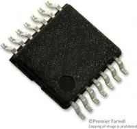
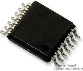
74LCX74MTCX, Триггер, дополнительный выход, положительный фронт, 74LCX74, D, 150 МГц, TSSOP
49,00 ₽
High-speed, 150MHz D flip-flop with clear/set, positive edge trigger, and complementary outputs. 5V tolerant, low EMI. Купить от FedExpert
The 74LCX74MTCX is a dual D-type Flip-flop with asynchronous clear and set inputs and complementary (Q, Q) outputs. Information at the input is transferred to the outputs on the positive edge of the clock pulse. After the clock pulse input threshold voltage has been passed, the data input is locked out and information present will not be transferred to the outputs until the next rising edge of the clock pulse input.
• 5V Tolerant inputs
• Power down high impedance inputs and outputs
• ±24mA Output drive current
• Implements proprietary noise/EMI reduction circuitry
• Latch-up performance exceeds JEDEC 78 conditions
Полупроводники — МикросхемыЛогикаТриггеры
Технические параметры
| Минимальная Рабочая Температура | -40 C |
| Максимальная Рабочая Температура | 85 C |
| Частота | 150МГц |
| Максимальное Напряжение Питания | 3.6В |
| Минимальное Напряжение Питания | 2В |
| Количество Выводов | 14вывод(-ов) |
| Тип Выхода Микросхемы | Дополнительный |
| Стиль Корпуса Микросхемы Логики | TSSOP |
| Тип Триггера | D, Положительный Фронт |
| Базовый Номер / Семейство Логики | 74LCX74 |
| Базовый Номер Микросхемы Логики | 7474 |
| Семейство Логической Микросхемы | 74LCX |
| Maximum Operating Temperature | +85 C |
| Number of Elements per Chip | 2 |
| Length | 5mm |
| Maximum Propagation Delay Time @ Maximum CL | 8ns |
| Minimum Operating Supply Voltage | 2 V |
| Brand | ON Semiconductor |
| Propagation Delay Test Condition | 50pF |
| Polarity | Inverting, Non-Inverting |
| Package Type | TSSOP |
| Mounting Type | Surface Mount |
| Minimum Operating Temperature | -40 C |
| Width | 4.4mm |
| Logic Family | LCX |
| Height | 0.9mm |
| Set/Reset | Yes |
| Logic Function | D Type |
| Output Type | 3 State |
| Triggering Type | Positive Edge |
| Maximum Operating Supply Voltage | 3.6 V |
| Pin Count | 14 |
| Dimensions | 5 x 4.4 x 0.9mm |
| Вес, г | 0.188 |
Похожие товары

ON Semiconductor
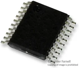
74VHC574MTCX, Триггер, на 3 состояния, положительный фронт, 74VHC574, D, 180 МГц, TSSOP
ON Semiconductor
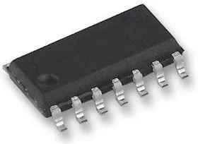
MC74HCT74ADR2G, Триггер, дополнительный выход, положительный фронт, 74HCT74, D, 24 нс, 30 МГц, NSOIC
ON Semiconductor
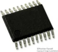
MC74LCX574DTR2G, Триггер, 74LCX574, D, 8.5 нс, 150 МГц, TSSOP